- 您现在的位置:买卖IC网 > Sheet目录3861 > PIC18F45K80-I/ML (Microchip Technology)MCU PIC 32KB FLASH 44QFN
2010-2012 Microchip Technology Inc.
DS39977F-page 111
PIC18F66K80 FAMILY
6.3.4
SPECIAL FUNCTION REGISTERS
The Special Function Registers (SFRs) are registers
used by the CPU and peripheral modules for controlling
the desired operation of the device. These registers are
implemented as static RAM. SFRs start at the top of
data memory (FFFh) and extend downward to occupy
all of Bank 15 (F00h to FFFh) and the top part of
Bank 14 (EF4h to EFFh).
A list of these registers is given in Table 6-1 and
The SFRs can be classified into two sets: those
associated with the “core” device functionality (ALU,
Resets and interrupts) and those related to the
peripheral functions. The Reset and Interrupt registers
are described in their respective chapters, while the
ALU’s STATUS register is described later in this section.
Registers related to the operation of the peripheral
features are described in the chapter for that peripheral.
The SFRs are typically distributed among the
peripherals whose functions they control. Unused SFR
locations are unimplemented and read as ‘0’s.
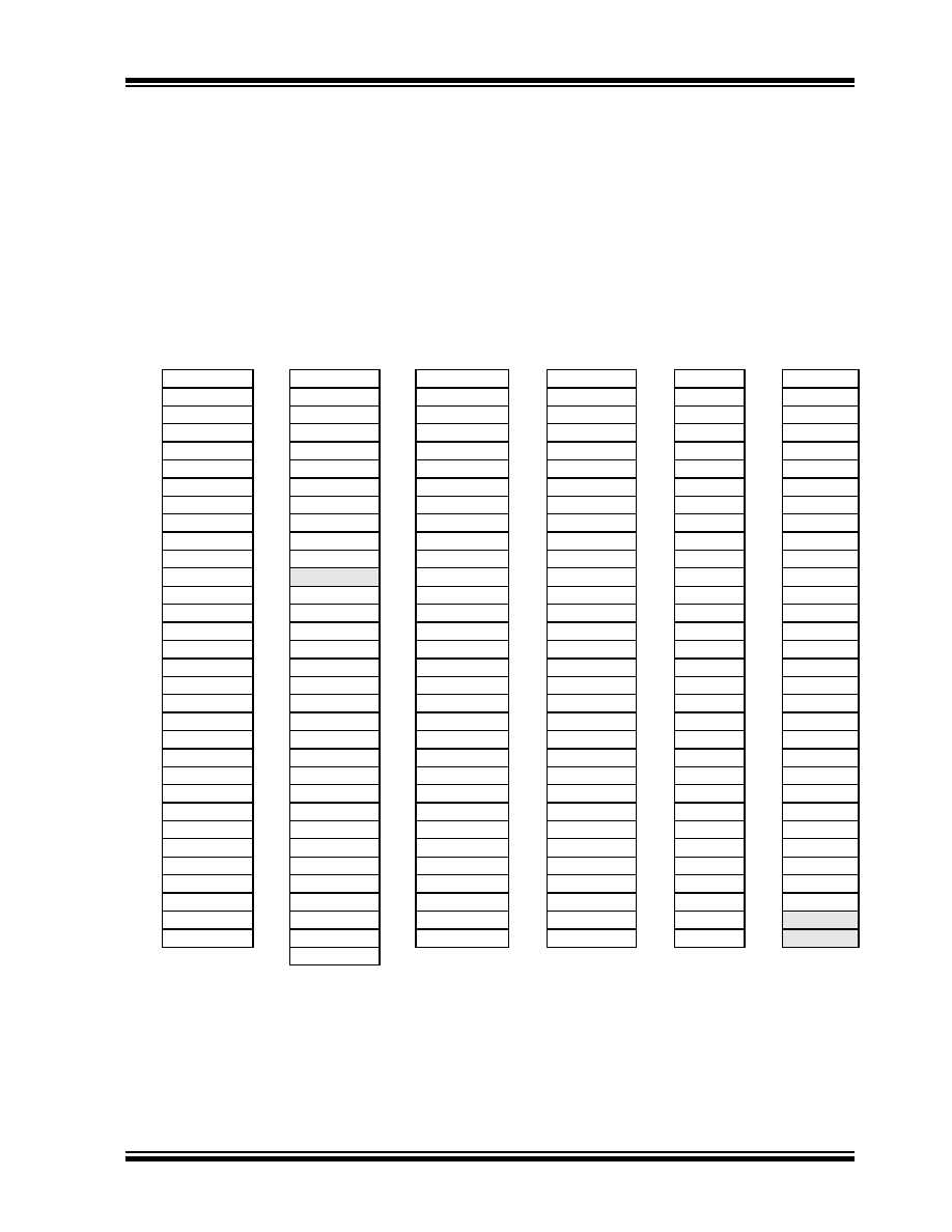
TABLE 6-1:
SPECIAL FUNCTION REGISTER MAP FOR PIC18F66K80 FAMILY
Addr.
Name
Addr.
Name
Addr.
Name
Addr.
Name
Addr.
Name
Addr.
Name
FFFh
TOSU
FDFh
INDF2(1)
FBFh
ECCP1AS
F9Fh
IPR1
F7Fh
EECON1
F5Fh CM1CON(5)
FFEh
TOSH
FDEh
POSTINC2(1)
FBEh
ECCP1DEL
F9Eh
PIR1
F7Eh
EECON2
F5Eh CM2CON(5)
FFDh
TOSL
FDDh
POSTDEC2(1)
FBDh
CCPR1H
F9Dh
PIE1
F7Dh SPBRGH1
F5Dh ANCON0(5)
FFCh
STKPTR
FDCh
PREINC2(1)
FBCh
CCPR1L
F9Ch
PSTR1CON
F7Ch SPBRGH2
F5Ch ANCON1(5)
FFBh
PCLATU
FDBh
PLUSW2(1)
FBBh
CCP1CON
F9Bh
OSCTUNE
F7Bh
SPBRG2
F5Bh
WPUB(5)
FFAh
PCLATH
FDAh
FSR2H
FBAh
TXSTA2
F9Ah
REFOCON
F7Ah
RCREG2
F5Ah
IOCB(5)
FF9h
PCL
FD9h
FSR2L
FB9h
BAUDCON2
F99h
CCPTMRS
F79h
TXREG2
F59h
PMD0(5)
FF8h
TBLPTRU
FD8h
STATUS
FB8h
IPR4
F98h
TRISG(3)
F78h
IPR5
F58h
PMD1(5)
FF7h
TBLPTRH
FD7h
TMR0H
FB7h
PIR4
F97h
TRISF(3)
F77h
PIR5
F57h
PMD2(5)
FF6h
TBLPTRL
FD6h
TMR0L
FB6h
PIE4
F96h
TRISE(4)
F76h
PIE5
F56h PADCFG1(5)
FF5h
TABLAT
FD5h
T0CON
FB5h
CVRCON
F95h
TRISD(4)
F75h
EEADRH
F55h CTMUCONH(5)
FF4h
PRODH
FD4h
—(2)
FB4h
CMSTAT
F94h
TRISC
F74h
EEADR
F54h CTMUCONL(5)
FF3h
PRODL
FD3h
OSCCON
FB3h
TMR3H
F93h
TRISB
F73h
EEDATA
F53h CTMUICONH(5)
FF2h
INTCON
FD2h
OSCCON2
FB2h
TMR3L
F92h
TRISA
F72h ECANCON
F52h CCPR2H(5)
FF1h
INTCON2
FD1h
WDTCON
FB1h
T3CON
F91h
ODCON
F71h COMSTAT
F51h
CCPR2L(5)
FF0h
INTCON3
FD0h
RCON
FB0h
T3GCON
F90h
SLRCON
F70h
CIOCON
F50h CCP2CON(4,5)
FEFh
INDF0(1)
FCFh
TMR1H
FAFh
SPBRG1
F8Fh
LATG(3)
F6Fh
CANCON
F4Fh CCPR3H(4,5)
FEEh
POSTINC0(1)
FCEh
TMR1L
FAEh
RCREG1
F8Eh
LATF(3)
F6Eh
CANSTAT
F4Eh CCPR3L(4,5)
FEDh
POSTDEC0(1)
FCDh
T1CON
FADh
TXREG1
F8Dh
LATE(4)
F6Dh
RXB0D7
F4Dh CCP3CON(5)
FECh
PREINC0(1)
FCCh
TMR2
FACh
TXSTA1
F8Ch
LATD(4)
F6Ch
RXB0D6
F4Ch CCPR4H(5)
FEBh
PLUSW0(1)
FCBh
PR2
FABh
RCSTA1
F8Bh
LATC
F6Bh
RXB0D5
F4Bh
CCPR4L(5)
FEAh
FSR0H
FCAh
T2CON
FAAh
T1GCON
F8Ah
LATB
F6Ah
RXB0D4
F4Ah CCP4CON(5)
FE9h
FSR0L
FC9h
SSPBUF
FA9h
PR4
F89h
LATA
F69h
RXB0D3
F49h CCPR5H(5)
FE8h
WREG
FC8h
SSPADD
FA8h
HLVDCON
F88h
T4CON
F68h
RXB0D2
F48h
CCPR5L(5)
FE7h
INDF1(1)
FC8h
SSPMSK
FA7h
BAUDCON1
F87h
TMR4
F67h
RXB0D1
F47h CCP5CON(5)
FE6h
POSTINC1(1)
FC7h
SSPSTAT
FA6h
RCSTA2
F86h
PORTG(3)
F66h
RXB0D0
FE5h
POSTDEC1(1)
FC6h
SSPCON1
FA5h
IPR3
F85h
PORTF(3)
F65h RXB0DLC
F45h MDCON(3,5)
FE4h
PREINC1(1)
FC5h
SSPCON2
FA4h
PIR3
F84h
PORTE
F64h RXB0EIDL
FE3h
PLUSW1(1)
FC4h
ADRESH
FA3h
PIE3
F83h
PORTD(4)
F63h RXB0EIDH
FE2h
FSR1H
FC3h
ADRESL
FA2h
IPR2
F82h
PORTC
F62h RXB0SIDL
FE1h
FSR1L
FC2h
ADCON0
FA1h
PIR2
F81h
PORTB
F61h RXB0SIDH
F41h
—(2)
FE0h
BSR
FC1h
ADCON1
FA0h
PIE2
F80h
PORTA
F60h RXB0CON
F40h
—(2)
FC0h
ADCON2
Note
1:
This is not a physical register.
2:
Unimplemented registers are read as ‘0’.
3:
This register is only available on devices with 64 pins.
4:
This register is not available on devices with 28 pins.
5:
Addresses, E41h through F5Fh, are also used by the SFRs, but are not part of the Access RAM. To access these registers, users must
always load the proper BSR value.
发布紧急采购,3分钟左右您将得到回复。
相关PDF资料
PIC24F32KA302-I/ML
MCU 32KB FLASH 2KB RAM 28-QFN
PIC18LF45K80-I/ML
MCU PIC ECAN 32KBFLASH 44QFN
PIC18F4221-I/PT
IC PIC MCU FLASH 2KX16 44TQFP
PIC18F1320-I/SO
IC MCU FLASH 4KX16 A/D 18SOIC
PIC18LF2321-I/SS
IC PIC MCU FLASH 4KX16 28SSOP
PIC16F917-I/PT
IC PIC MCU FLASH 8KX14 44TQFP
PIC18F1320-I/SS
IC MCU FLASH 4KX16 A/D 20SSOP
PIC24FV32KA301-I/P
MCU 32KB FLASH 2KB RAM 20-PDIP
相关代理商/技术参数
PIC18F45K80-I/P
功能描述:8位微控制器 -MCU 32KB FL 4KBRM 16MIPS 12bit ADC CTMU RoHS:否 制造商:Silicon Labs 核心:8051 处理器系列:C8051F39x 数据总线宽度:8 bit 最大时钟频率:50 MHz 程序存储器大小:16 KB 数据 RAM 大小:1 KB 片上 ADC:Yes 工作电源电压:1.8 V to 3.6 V 工作温度范围:- 40 C to + 105 C 封装 / 箱体:QFN-20 安装风格:SMD/SMT
PIC18F45K80-I/PT
功能描述:8位微控制器 -MCU 32KB FL 4KBRM 16MIPS 12bit ADC CTMU RoHS:否 制造商:Silicon Labs 核心:8051 处理器系列:C8051F39x 数据总线宽度:8 bit 最大时钟频率:50 MHz 程序存储器大小:16 KB 数据 RAM 大小:1 KB 片上 ADC:Yes 工作电源电压:1.8 V to 3.6 V 工作温度范围:- 40 C to + 105 C 封装 / 箱体:QFN-20 安装风格:SMD/SMT
PIC18F45K80T-I/ML
功能描述:8位微控制器 -MCU 32KB FL 4KBRM 16MIPS 12bit ADC CTMU RoHS:否 制造商:Silicon Labs 核心:8051 处理器系列:C8051F39x 数据总线宽度:8 bit 最大时钟频率:50 MHz 程序存储器大小:16 KB 数据 RAM 大小:1 KB 片上 ADC:Yes 工作电源电压:1.8 V to 3.6 V 工作温度范围:- 40 C to + 105 C 封装 / 箱体:QFN-20 安装风格:SMD/SMT
PIC18F45K80T-I/PT
功能描述:8位微控制器 -MCU 32KB FL 4KBRM 16MIPS 12bit ADC CTMU RoHS:否 制造商:Silicon Labs 核心:8051 处理器系列:C8051F39x 数据总线宽度:8 bit 最大时钟频率:50 MHz 程序存储器大小:16 KB 数据 RAM 大小:1 KB 片上 ADC:Yes 工作电源电压:1.8 V to 3.6 V 工作温度范围:- 40 C to + 105 C 封装 / 箱体:QFN-20 安装风格:SMD/SMT
PIC18F4610-E/ML
功能描述:8位微控制器 -MCU 64KB 3968 RAM 36 I/O RoHS:否 制造商:Silicon Labs 核心:8051 处理器系列:C8051F39x 数据总线宽度:8 bit 最大时钟频率:50 MHz 程序存储器大小:16 KB 数据 RAM 大小:1 KB 片上 ADC:Yes 工作电源电压:1.8 V to 3.6 V 工作温度范围:- 40 C to + 105 C 封装 / 箱体:QFN-20 安装风格:SMD/SMT
PIC18F4610-E/P
功能描述:8位微控制器 -MCU 64KB 3968 RAM 36 I/O RoHS:否 制造商:Silicon Labs 核心:8051 处理器系列:C8051F39x 数据总线宽度:8 bit 最大时钟频率:50 MHz 程序存储器大小:16 KB 数据 RAM 大小:1 KB 片上 ADC:Yes 工作电源电压:1.8 V to 3.6 V 工作温度范围:- 40 C to + 105 C 封装 / 箱体:QFN-20 安装风格:SMD/SMT
PIC18F4610-E/PT
功能描述:8位微控制器 -MCU 64KB 3968 RAM 36 I/O RoHS:否 制造商:Silicon Labs 核心:8051 处理器系列:C8051F39x 数据总线宽度:8 bit 最大时钟频率:50 MHz 程序存储器大小:16 KB 数据 RAM 大小:1 KB 片上 ADC:Yes 工作电源电压:1.8 V to 3.6 V 工作温度范围:- 40 C to + 105 C 封装 / 箱体:QFN-20 安装风格:SMD/SMT
PIC18F4610-I/ML
功能描述:8位微控制器 -MCU 64KB 3968 RAM 36 I/O RoHS:否 制造商:Silicon Labs 核心:8051 处理器系列:C8051F39x 数据总线宽度:8 bit 最大时钟频率:50 MHz 程序存储器大小:16 KB 数据 RAM 大小:1 KB 片上 ADC:Yes 工作电源电压:1.8 V to 3.6 V 工作温度范围:- 40 C to + 105 C 封装 / 箱体:QFN-20 安装风格:SMD/SMT